The bottleneck limiting the next generation of artificial intelligence isn’t compute power—it’s the wire connecting the chips. French startup Scintil Photonics thinks it has the answer.
For decades, the semiconductor industry operated on a comforting assumption: as chips grew faster, the rest of the system would keep pace. That assumption is now breaking down, and nowhere is the stress more visible than inside an AI data center.
The numbers are staggering. Cloud bandwidth demand effectively doubles every two years. AI model sizes are scaling faster than Moore’s Law can accommodate. Jensen Huang, Nvidia’s CEO, captured the magnitude of the challenge at Computex 2025 when he remarked that the NVLink spine—the high-speed interconnect fabric linking Nvidia’s GPU clusters—moves more data per second than the entire internet. What was once a theoretical constraint has become an operational emergency.
Copper Hitting Its Limits
The culprit is copper. Traditional copper SerDes interconnects have served the industry reliably for years, but they are hitting fundamental physical limits. At the signal speeds modern AI workloads demand, copper cables can only span short distances before signal integrity collapses.
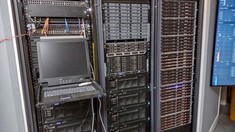
With GPU clusters continuing to scale upwards, copper interconnects are struggling to keep pace. Image used courtesy of Adobe Stock (licensed).
As GPU clusters expand from dozens to hundreds to thousands of accelerators spread across multiple racks, copper simply cannot bridge the gap. The AI scale-up networks of tomorrow—the dense, high-bandwidth fabrics that allow thousands of GPUs to coordinate as a single computational entity—require something fundamentally different.
That something is light. The photonics industry has long supplied optical transceivers to data centers in the form of pluggable modules—discrete components that convert electrical signals to optical ones at the edge of a switch or server. These pluggable solutions work, but they come with a steep cost: latency measured in tens to hundreds of nanoseconds, energy consumption around 17–18 picojoules per bit, and bandwidth density that tops out around 1–2 terabits per second per millimeter of chip edge.
For the next generation of AI infrastructure, those numbers are inadequate by an order of magnitude.
Co-Packaged Optics
The emerging solution is co-packaged optics (CPO)—integrating the optical engine directly alongside the compute ASIC or GPU on the same substrate, eliminating the long electrical trace between processor and transceiver. But not all CPO architectures are equal. The mainstream approach uses CWDM (Coarse Wavelength Division Multiplexing), which packs four optical channels onto a fiber at up to 200 Gbps per channel. It improves on pluggables, but it’s a half-measure.
The more promising architecture—and the one that Scintil Photonics is betting the company on—is DWDM CPO: Dense Wavelength Division Multiplexing combined with co-packaged integration. The performance gap between the two is stark. Where CWDM CPO delivers latency of 50 to 100 nanoseconds and energy efficiency around 7 picojoules per bit, DWDM CPO achieves latency below 5 nanoseconds and energy efficiency under 3.5 picojoules per bit.
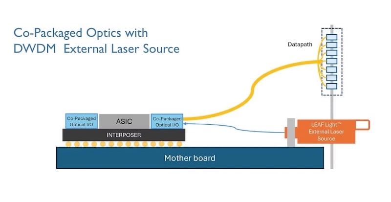
Scintil’s approach is to combine DWDense Wavelength Division Multiplexing (DWPM) with co-packaged integration.
Bandwidth density scales to more than 8 terabits per second per millimeter—roughly eight times that of CWDM CPO—and a single fiber can carry up to 1,600 Gbps. When measured against legacy pluggables, DWDM CPO delivers a 6x reduction in power consumption.
The catch is that DWDM CPO requires something the photonics industry has never successfully produced at volume: a single-chip, multi-wavelength laser source that can be fabricated directly on a standard silicon photonics wafer.
Silicon Photonics Tradoffs
Silicon photonics is an elegant idea with a stubborn limitation. Silicon is an excellent medium for routing and modulating light, but it cannot efficiently generate it. Lasers, the light sources at the heart of any optical interconnect, are traditionally made from III-V semiconductor materials—compounds like indium phosphide—which are chemically and structurally incompatible with standard silicon manufacturing processes.
The conventional workaround is to build the laser separately and attach it to the silicon photonic chip, either by bonding a discrete die or connecting an external module. This works, but it reintroduces the integration penalty that CPO was supposed to eliminate: extra interfaces mean more loss, more power, more failure modes, and dramatically higher cost at volume.
Grenoble-based Scintil Photonics was founded in France to solve this integration problem from first principles. The company’s core innovation is the SHIP process—Scintil Heterogeneous Integrated Photonics—a wafer-level fabrication technique that allows III-V laser material to be integrated directly onto a standard silicon photonics platform.
An Elegant Approach
The process is elegant in its approach. Scintil begins with a standard silicon photonic wafer containing the passive and active components—waveguides, modulators, photodetectors—fabricated using conventional CMOS-compatible processes. The original silicon-on-insulator substrate is then removed via a handle exchange, exposing the buried oxide layer.
Unpatterned III-V semiconductor dice are bonded to this surface precisely where the lasers will reside. Critically, the III-V material is then patterned using photolithography at the wafer level—the same manufacturing step that defines the laser wavelengths—giving Scintil exceptional precision over wavelength control that discrete assembly cannot match.
The result is a monolithically integrated chip where lasers, waveguides, modulators, and detectors coexist on a single piece of silicon, manufactured in a single fab flow.
Scintil’s LEAF Light
Scintil’s first commercial product, the LEAF Light, is the world’s first single-chip DWDM laser source designed for AI-scale co-packaged optics. It supports configurations of 8 or 16 wavelengths on a single chip, with frequency spacing precision of ±10 GHz—the tightest in the industry. Each wavelength carrier delivers up to 20 milliwatts of optical power, with wall-plug efficiency of approximately 20% at operating temperature.
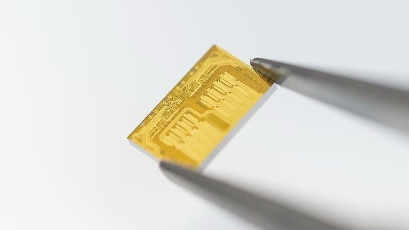
LEAF Light is a single-chip DWDM laser source designed for AI-scale co-packaged optics.
Critically for data center operators, LEAF Light eliminates the failure modes most commonly associated with high-speed lasers. By removing the need for anti-reflection coatings and avoiding current flow through the grating structure, the architecture achieves stable, mode-hop-free operation. This reliability characteristic matters enormously at the scale of modern AI infrastructure, where a single failed optical component can degrade the performance of an entire GPU cluster.
The market opportunity is substantial. Scintil estimates the 2030 serviceable addressable market for LEAF Light at approximately $4.9 billion, based on projected XPU shipment volumes of 31 million units by the end of the decade, with an average attach rate of two DWDM light sources per accelerator.
Financial Signals
In September 2025, Scintil closed a Series B funding round raising $58 million—part of a total capitalization of $85 million USD. The round was co-led by Yotta and Nokia Growth Partners, with participation from Nvidia, and saw 100% reinvestment from existing backers including Bpifrance, Supernova Invest, Bosch Venture Capital, Applied Ventures, and ITIC-Taiwan. The round was significantly oversubscribed.
Scintil’s A Series B investment round, spearheaded by Yotta Capital Partners and NGP Capital, featured significant participation from Nvidia.
Nvidia’s participation is more than a financial signal. It indicates that the world’s dominant GPU maker—whose scale-up interconnect fabric is at the center of every major AI infrastructure build—sees heterogeneous integrated photonics as a credible path forward.
Scintil’s production roadmap calls for the LEAF Light product launch and pilot production this year in 2026, with early-access customer shipments beginning the same year and volume production ramping through 2027. The company has a high-volume manufacturing partnership with Tower Semiconductor, one of the leading silicon photonics foundries, providing the fab capacity necessary to scale to over 100 million units.
Not If But When
The physics is clear. Copper is not going to scale to the bandwidth densities that AI infrastructure demands. The transition to optical interconnects is no longer a question of if—it is a question of which architecture, at what cost, from whom. Scintil’s bet is that the answer begins with a single chip, sixteen wavelengths, and a manufacturing process that finally makes light native to silicon.
All images used courtesy Scintil, except where specified otherwise.