FR-4 is a family of laminates, not a single material. Learn how dielectric variation and loss determine performance and identify when it stops working for fast digital designs.
The materials in a PCB stackup are the foundation for any new electronic product, and yet so many designers refuse to take ownership of this aspect of PCB design.
The most common category of materials used in PCB builds is FR-4, or more specifically, flame retardant type-4 materials. This material set is the basis for most mass-produced electronics due to its huge range of applicability and wide range of compositions. FR-4 designs also enjoy use in what would often be considered “advanced” designs, such as those involving large digital processors and other advanced semiconductors.

High-speed PCB designs may require more than FR-4.
Despite the widespread usage of FR-4 materials, many designers simply allow the fabrication house to supply a standard stackup or pick the materials. Not all designs require this level of control and detail, but for those that do, the designer should take ownership of the material selection. This can make the difference between a design that is solvable and a design where the FR-4 materials eliminate any routing freedom.
What Is FR-4 Material in PCBs?
Many designers don’t realize until they start comparing standard stackups from manufacturers that FR-4 doesn’t refer to a specific material. FR-4 is a broad designation from the National Electrical Manufacturers Association (NEMA) and an acronym for flame-retardant type 4. Broadly, any epoxy resin-based composite material that meets the NEMA definition could be considered FR-4.
Many manufacturers of circuit board materials produce laminates that meet the FR-4 classification. In terms of their internal structure and base materials, they all have common characteristics:
- Woven fiberglass cloth reinforcement bonded with an epoxy resin system
- Flame retardancy meeting UL 94 V-0 requirements
- Copper-clad surfaces suitable for etching and plating during PCB fabrication
- Available in standard thicknesses and copper weights compatible with multilayer lamination processes
- Dielectric properties sufficient for controlled-impedance routing at moderate frequencies
- Mechanical rigidity adequate for component mounting, soldering, and board-level assembly
- Thermal performance characterized by glass transition temperature, decomposition temperature, and z-axis expansion behavior
While there are many possible base materials that can be used to design and manufacture an FR-4 laminate, the main materials are woven fiberglass, epoxy resin filler, flame retardant additives, and a curing agent.
Common materials used to build an FR-4 laminate.
| Material Category | Specific Chemicals or Product Names |
| Woven fiberglass | E-glass cloth (styles 106, 1080, 2116, 7628), S-glass, NE-glass (low-Dk glass) |
| Epoxy resin filler | DGEBPA (diglycidyl ether of bisphenol A), DGEBPF (diglycidyl ether of bisphenol F), multifunctional epoxy blends, phenolic-cured epoxy systems |
| Flame retardant additives | TBBPA (tetrabromobisphenol A), phosphorus-based flame retardants, aluminum hydroxide fillers, halogen-free reactive flame retardants |
| Curing agent | Dicyandiamide (DICY), phenolic novolac hardeners, aromatic amine hardeners |
The NEMA definition of FR-4 covers general properties like flexural strength, bond strength, moisture absorption, arc resistance, and dielectric breakdown voltage. These parameters qualify FR-4 for non-PCB electrical insulation applications like terminal boards and switchgear. While PCB designers rarely reference these properties directly, they form the baseline distinguishing FR-4 from other material grades explicitly defined by NEMA.
What Materials Are Classified as FR-4?
There are many commercial materials that meet the definition of FR-4, and they are sold under many brand names. While it is difficult to estimate the number of materials currently sold and stocked in the PCB supply chain, there are certainly hundreds of distinct laminate formulations that have been manufactured and sold commercially. These laminate formulations vary in terms of their base materials (see the table above). These base materials give each formulation its particular process compatibility, electrical properties, and mechanical properties.
Going further, FR-4 is often subdivided into two different categories: standard FR-4 and advanced FR-4. These are mostly marketing terms; there is no industry standard that specifically defines “standard” or “advanced” FR-4. These are primarily delineated by the dielectric constant. An advanced FR-4 material tends to have a lower Dk value and a corresponding lower loss tangent.
Typical properties of standard and advanced FR-4 materials.
| Standard FR-4 |
|
| Advanced FR-4 |
|
The IPC-4101 standard classifies FR-4 materials using “slash sheets” (e.g., /21, /24) to identify substitutes with compatible resin systems, reinforcement types, and process requirements. While materials under the same slash sheet can be interchanged during lamination, drilling, and plating without workflow changes, their electrical properties like Dk and loss tangent may still vary. Designers must ensure any substitution fulfills the specific electrical requirements of the design.
Process compatibility table from IPC-4101. Used courtesy of the Global Electronics Association
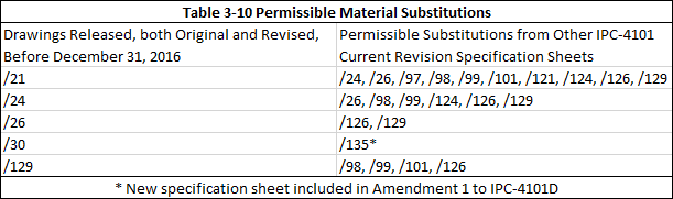
When a designer decides to specify the particular FR-4 materials in their stackup, they can call out one of the following in their fabrication notes:
- The commercial product name and laminate weave data
- The IPC-4101 slash sheet number
- A generic callout with an acceptable Dk and/or thickness range
Fabrication notes are the most obvious place to call out the slash sheet number and/or commercial name for a particular material. For example, in Altium Draftsman, users can place custom fabrication notes alongside standard fabrication drawing features like hole schedules, drill drawings, and layer plots. This approach places the auto-generated fabrication data in a master drawing alongside the custom notes for the manufacturer. It is one of the most common ways to specify materials when controlled impedance is not required.
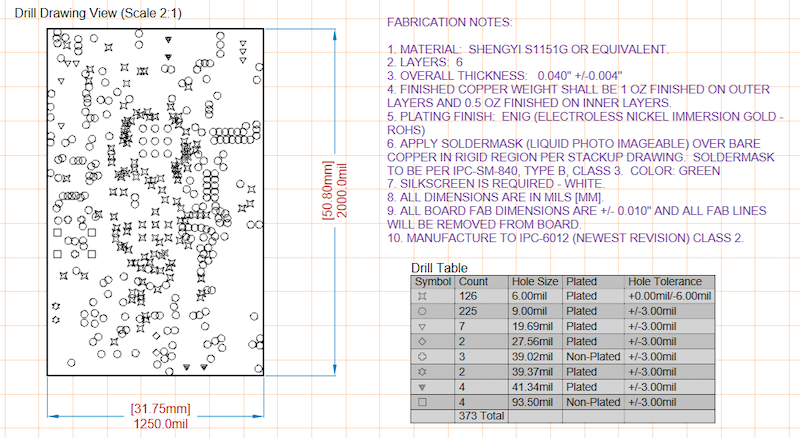
Fabrication drawing with custom fabrication notes in Altium Draftsman.
The designer should still check other performance parameters of the material before finalizing it for a design. These could include glass transition temperature (Tg), breakdown strength (for high-voltage designs), CTE values, and mechanical moduli. For more specialized designs, like HDI designs, the material will need to be laser-drillable for placement of microvias.
Dk Variation With Frequency
All materials, whether natural, engineered, or composite, will exhibit dispersion over broad frequency ranges. Dispersion refers to a change in a material property, in this case the dielectric constant, over frequency. However, over very limited frequency ranges, dielectric constant dispersion can be small or very near zero. This is the condition that some FR-4 materials manufacturers have attempted to engineer into their products.
Unfortunately, one only needs to look at a PCB material datasheet to see just how successful materials manufacturers have been in this endeavor. Dispersion can change the dielectric constant by up to 10% from 100 MHz to 10 GHz. This variation increases the transmission line impedance by approximately 5%. That is before accounting for other sources of loss in the channel (dielectric loss, skin effect, and roughness).
How does FR-4 dielectric constant change with frequency? Some examples showing the variation in Isola 370HR, a popular advanced FR-4 laminate option, is given in the image below.
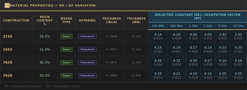
Sample dielectric constant data for Isola 370HR prepreg offerings.
For many digital interfaces, including high-speed interfaces with channel bandwidths up to 1 GHz, this variation is insignificant. For example, gigabit Ethernet will work and will achieve channel compliance on the above 370HR laminate options. However, a design with 10Gbps SerDes has a much higher chance of failure due to the dielectric variation. The impedance deviation creates more return loss at higher frequencies.
However, if we can reduce the dielectric constant variation, as well as reduce dielectric losses, we can extend the range where the standard lossless impedance calculations are reliable. These calculations are implemented in PCB design software. This is why more advanced materials are used when higher channel bandwidths are required on digital interfaces.
Beyond FR-4 With Advanced Materials
More advanced materials than those marketed as “advanced FR-4” are available for high-speed designs and RF designs. Many of these are laser-drillable, which means they can also support high-density designs, as well as additive processing for ultra-high-density designs. Common product/brand names include Tachyon 100G, Megtron, EMC 800, Rogers, and Panasonic LCP.
High-speed PCB designs and IC substrate designs requiring channel bandwidths at 10 GHz or higher routinely make use of these advanced materials due to their lower Dk value, lower loss tangent, lower dispersion, and compatibility with standard processing. These materials can also be integrated with standard FR-4 materials to build hybrid stackups. The right layer ordering must be selected in the stackup to ensure strong bonding between layers.
Whatever style stackup you plan to build, it needs to be specified in your PCB software, including the material thicknesses, product name, and dielectric properties. As an example, the Layer Stack Manager in Altium Designer gives exactly this level of control for material definitions. Once the PCB stackup materials are defined, the information can be immediately imported into an automated stackup drawing in Altium Draftsman. This provides the exact documentation a manufacturer needs to build the PCB.
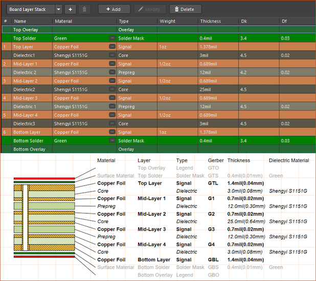
Top: PCB stackup definition in Altium Designer.
Bottom: Automatically generated stackup drawing for fabrication in Altium Draftsman.
Whether a high-speed PCB will need standard/advanced FR-4 or a more advanced material, the material selection can be qualified in the stackup with a simple design process:
- Determine trace sizing/spacing for impedance-controlled lines in each layer and verify manufacturer capabilities can fabricate this value
- Send the proposed stackup to the fabrication house to ensure materials are stocked/available
- If the stackup is updated by the manufacturer, put the new data into the PCB stackup design and determine the new trace sizing/spacing
- Check the new sizing/spacing against the clearance and layer constraints in fanout routing (if applicable)
This ensures the manufacturer has a chance to review this critical area of a design before the layout is completed. The risk of re-design is effectively reduced, and the designer can proceed to routing with high confidence.
Except where noted, all images are used courtesy of Altium.