France’s Électronique 2030 program commits €5B+ to revitalize its semiconductor industry. Learn the details of this ambitious effort, and the market challenges it’s facing.
The central government in Paris is deploying billions to anchor next-generation chip manufacturing on French soil. The moves stretch across a broad spectrum, from the Grenoble megafab to silicon photonics and power electronics—but ambitious plans are already meeting market headwinds.
The Électronique 2030 Framework: Policy Architecture and Funding Commitments
France’s most consequential recent act of semiconductor industrial policy is the Électronique 2030 program, launched by President Emmanuel Macron in July 2022 during a visit to STMicroelectronics’ fabrication site in Crolles, Isère. The program sits within the broader France 2030 investment plan—a €54 billion, ten-sector strategy for industrial reinvention—and commits more than €5 billion in direct state support to the electronics value chain through 2030. That public anchor is designed to catalyze total investment of some €16 billion, with the creation of an estimated 5,700 direct jobs.
The Électronique 2030 program, launched in 2022, is part of the broader France 2030 initiative. Image used courtesy of info.gouv.fr.
The policy rationale is explicitly sovereign. France—and by extension Europe—once produced close to 40 percent of global semiconductor output; that share has collapsed to under 10 percent, leaving automotive, defense, and consumer electronics supply chains exposed to geopolitical shocks, as the COVID-19 disruptions painfully demonstrated. Électronique 2030 is conceived as a structural corrective across three axes: expanding manufacturing capacity, intensifying frontier R&D, and building the workforce pipeline that advanced fabs require.
Two Funding Mechanisms
The program’s architecture draws on two interlocking funding mechanisms. Domestically, the state investment bank Bpifrance administers grants, co-investment vehicles, and the France 2030 i-Demo innovation program.
At the European level, France participates in the Important Project of Common European Interest for Microelectronics and Communications Technologies (PIIEC ME/CT), a 20-member-state framework under which 15 French industrial leaders—including STMicroelectronics, Soitec, Lynred, Teledyne e2v, Aledia, and Kalray—receive structured EU-compatible state aid for qualifying R&D and pilot production. The PIIEC model allows member states to bypass standard state-aid ceilings when supporting strategically vital and innovation-additive projects, an instrument France lobbied hard to establish.
Research funding received a significant dedicated allocation: €800 million for academic and applied R&D, channeled primarily through CEA-Leti in Grenoble, and €50 million for training programs to expand the pool of electronics engineers. The workforce clause is notable—individual grant disbursements are tied to the creation of new vocational-training slots, meaning that capital and talent formation are co-managed rather than siloed.
Key Transactions and Technology Bets: Fabs, Substrates, Photonics
The Crolles Megafab: Flagship Investment, Contested Progress
The headline investment in Électronique 2030 was the announcement of a new 300 mm fabrication facility in Crolles, to be built and jointly operated by STMicroelectronics and GlobalFoundries (GF). The project carried a combined capex, maintenance, and ancillary budget of approximately €7.5 billion, with the French state contributing around €2.9 billion—the largest semiconductor manufacturing subsidy in French history and one of the largest in Europe. The European Commission approved the aid in April 2023 under the EU Chips Act’s First-of-a-Kind facility provisions.
The technical focus is fully depleted silicon-on-insulator (FD-SOI) technology, which STMicroelectronics and CEA-Leti have pioneered over two decades in the Grenoble basin. FD-SOI offers a compelling combination of low power consumption, high RF performance, and comparatively simplified manufacturing, making it well suited for automotive microcontrollers, industrial IoT, 5G infrastructure, and edge-AI applications.
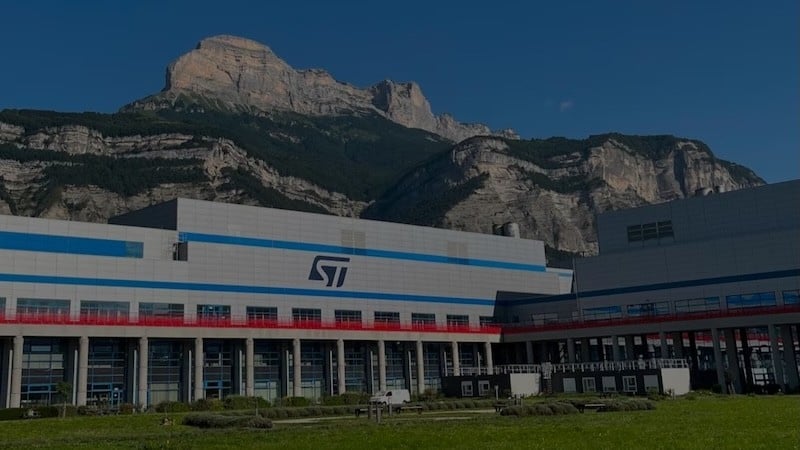
STMicro’s Crolles, France fab location. Image used courtesy of STMicroelectronics.
The joint facility was intended to scale this process to 18 nm class nodes, qualifying France for the global top-five in advanced manufacturing technology. When fully ramped, the site was projected to produce 14,000 300 mm wafers per week by 2027, with modular expansion pathways to 20,000.
The picture has grown more complicated since 2023. By mid-2025, GlobalFoundries had quietly decelerated its participation, citing market conditions and customer-demand uncertainty. Bloomberg reported the joint project as effectively shelved, and industry observers noted that the stall exposed a structural weakness in European Chips Act governance: once state aid is locked to a specific project, redeployment to alternative semiconductor initiatives requires restarting the full approval cycle. EE Times Europe found that the Grésivaudan Valley—home not only to ST and Soitec but to a dense network of supplier firms—had already re-allocated planned hiring in anticipation of the megafab’s ramp.
Despite the GF partnership’s pause, STMicroelectronics has continued to invest in Crolles independently. In April 2025, the company announced a restructuring of its global manufacturing footprint that reinforces France as its digital products hub: the existing 300 mm Crolles fab is to expand capacity to 14,000 wafers per week by 2027, while the adjacent 200 mm fab will be converted to advanced packaging and electrical wafer sorting—activities that, ST notes, do not currently exist elsewhere in Europe. The Crolles 200 mm line will also concentrate next-generation optical sensing and silicon photonics development, positioning the site as a European center for heterogeneous integration even as the wider megafab program stalls.
Soitec: The Substrate Supplier as National Champion
One of the most consequential, if less visible, nodes in France’s semiconductor ecosystem is Soitec, headquartered in Bernin, adjacent to Crolles. The company’s proprietary Smart Cut wafer-bonding process gives it a dominant position—approximately 70–80 percent of global market share—in silicon-on-insulator substrates, the foundational material for FD-SOI devices, RF-SOI for mobile handsets, and Photonic SOI for silicon photonics. Soitec generated sales of approximately €1 billion in fiscal year 2023–2024, and its 300 mm fab in Bernin is undergoing capacity expansion to meet AI-driven demand for photonic-grade wafers.

Bernin 2 is Soitec’s 300 mm fab in Bernin, France. Image used courtesy of Soitec.
Bpifrance has co-financed Soitec’s capacity expansion under Électronique 2030, funding the Bernin facility upgrade as a strategic complement to the Crolles manufacturing cluster. The company’s emerging SmartSiC substrate technology—applying Smart Cut to silicon carbide—is also under development with France 2030 support, targeting the automotive power electronics market where demand for SiC devices is surging alongside electrification mandates.
Silicon Photonics and Optics: The CanopAI Initiative
Among France’s more recent technology bets, the CanopAI consortium stands out as an indicator of how Électronique 2030 is now funding adjacent photonic industries. Awarded in January 2026 under Bpifrance’s France 2030 i-Demo program, the initiative brings together Scintil Photonics—a CEA-Leti spinout from Grenoble—with semiconductor testing and industrialization specialist Presto Engineering, and CEA-Leti itself. The project targets a new generation of photonic integrated circuits (PICs) for AI data-center interconnects, aiming to double transmission throughput every two years and dramatically improve energy efficiency at scale.
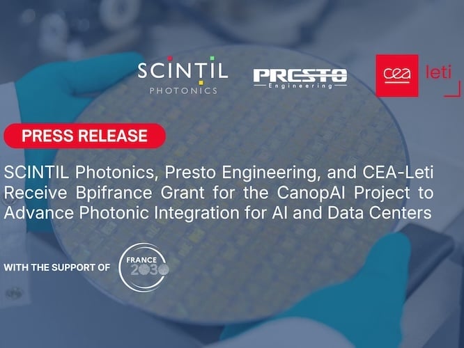
In January, Scintil, Presto Engineering and CEA-Leti received a Bpifrance grant for the CanopAI Project to advance photonic integration for AI and data centers. Image used courtesy of Scintil.
Scintil’s LEAF Light platform, a single-chip dense-wavelength-division-multiplexing light engine targeting speeds above one terabit per second, illustrates how France’s chip-adjacent optical and photonics competencies are being deliberately cultivated into production-ready technologies. The company raised €50 million in Series B funding in September 2025, building on CEA-Leti’s silicon photonics platform and the proximity of Soitec’s photonic-grade SOI wafer supply. For more on Scintil, check out my recent article here on All About Circuits.
The CanopAI grant also intersects with a broader June 2024 initiative: the FAMES Pilot Line, an €830 million cross-European project under the Chips Joint Undertaking, launched in the Grenoble-Crolles area. FAMES (Fabrication Advanced Manufacturing and Equipment for Semiconductor) aligns with the EU Chips Act’s bold ambition to establish shared, pre-commercial pilot-line infrastructure accessible to fabless design houses and SMEs. France hosts one of the program’s principal nodes, leveraging CEA-Leti’s 300 mm cleanroom and its decades of heterogeneous integration expertise.
Beyond the Megafab: Power Electronics, Defence, and Regional Ecosystems
Électronique 2030’s scope extends beyond large-node digital chips. France has made targeted commitments to gallium nitride (GaN) and silicon carbide (SiC) power semiconductors, which are essential for automotive inverters, renewable-energy conversion, and defense electronics. Renault and STMicroelectronics are jointly developing SiC traction inverters expected to reduce power losses by approximately 45 percent in next-generation electric drivetrains. Valeo and Vitesco Technologies both receive PIIEC funding for power electronics R&D, situating automotive system integrators within the national semiconductor value chain rather than treating them purely as downstream customers.
Defense and dual-use applications receive parallel attention. Teledyne e2v Semiconductors, based in Elancourt, is supported as a PIIEC industrial lead for high-reliability analogue and imaging devices used in space and defence. Lynred—a joint venture between Thales and Safran—produces cooled and uncooled infrared focal-plane arrays from its Grenoble facility, with Électronique 2030 support for next-generation sensor process development. Aledia, another Grenoble-based firm, is scaling 3D nanowire microLED production on silicon—a France 2030-backed technology with applications in next-generation displays and photonic systems.
At the sub-national level, the Auvergne-Rhône-Alpes region has been particularly active in co-funding cluster development. The Minalogic competitiveness cluster, which has facilitated coordination among the Grenoble-area microelectronics ecosystem for over 15 years, acts as a program intermediary, helping SMEs and ETIs access France 2030 calls for projects and PIIEC supply-chain integration. The region’s combination of Alpine hydroelectric power, engineering universities, and a 70-plus site network of fab-adjacent SMEs gives the Crolles-Bernin corridor structural advantages in per-wafer cost and talent retention that public policy is designed to reinforce.
Assessment: Strengths, Stress Points, and the Sovereignty Paradox
France’s semiconductor and advanced electronics strategy is coherent, well-funded, and architecturally sophisticated relative to most European peers. The policy intelligently targets a niche-focused model—exploiting France’s genuine structural advantages in FD-SOI, SOI substrates, silicon photonics, infrared sensing, and power electronics—rather than attempting to replicate the commodity-volume foundry models of Taiwan or South Korea.
CEA-Leti’s cooperative R&D model, in which government-funded research is closely co-developed with industrial partners before technology transfer, has become an internationally recognized template: a 2024 CSIS paper described it as a distinctive French contribution to the global semiconductor R&D ecosystem.
The stress points are real, however. The partial collapse of the Crolles megafab project is the most significant setback, and it illustrates a governance vulnerability inherent in the European Chips Act’s state-aid architecture: project-specific approval processes are slow and inflexible, unable to redeploy capital when market cycles shift. The lesson for France is that its dependence on a single flagship manufacturing investment—and on a single US industrial partner willing to build in Europe—created fragility that a more distributed investment portfolio might have avoided.
There is also a tension between the program’s sovereignty rhetoric and the operational reality of France’s semiconductor industry. STMicroelectronics is a Franco-Italian public company headquartered in Geneva. GlobalFoundries is a US firm. Soitec, while French-listed, operates fabs in Singapore and relies on global supply chains.
The fabless cluster—SiPearl, Kalray, Scintil—depends on TSMC or Samsung for advanced fabrication. Genuine French-sovereign manufacturing capability remains narrow, concentrated in FD-SOI mid-range nodes and specialty devices. The government’s stated ambition of achieving 10 nm-class domestic production—which would place France in the global top five—remains unrealized and will require either reviving the GF partnership, attracting a new foundry partner, or a dramatically elevated level of public investment.
The Outlook Ahead
On balance, France’s electronics industrial policy represents one of Europe’s more credible attempts at technology sovereignty. The Grenoble-Crolles corridor is a genuine world-class cluster; the PIIEC instrument has successfully mobilized a 15-firm national supply-chain program; and the emerging photonics and power-electronics pipeline is building value in segments where French firms already hold defensible positions.
The challenge for the remainder of the decade will be converting that R&D leadership into sustained, high-volume manufacturing—and maintaining fiscal commitment to the program in an era of constrained government budgets and shifting industrial alliances.
Sidebar: Key Milestones: France Semiconductor & Advanced Electronics Policy
Oct 2021—France 2030 investment plan launched (€54bn total, 10 sectors)
Jul 2022—Électronique 2030 unveiled at Crolles; €5bn+ state commitment; STMicro/GF megafab announced (€7.5bn total project cost)
Apr 2023—European Commission approves €2.9bn French aid for STMicro/GF Crolles fab under EU Chips Act
Jun 2024—FAMES Pilot Line launched in Grenoble-Crolles area (€830m EU Chips JU project)
Oct 2024—STMicroelectronics announces global manufacturing restructure; Crolles reaffirmed as core digital products hub
Oct 2024—France 2030 stratégie électronique update published by Direction Générale des Entreprises
Mid-2025—GlobalFoundries slows participation in Crolles megafab; joint project effectively paused
Sep 2025—Scintil Photonics raises €50m Series B; France 2030 i-Demo photonics pipeline expands
Jan 2026—CanopAI consortium (Scintil, Presto, CEA-Leti) awarded Bpifrance grant for AI photonic interconnects
Apr 2026—STMicroelectronics confirms Crolles 300mm ramp to 14,000wpw by 2027; 200mm fab to host advanced packaging and silicon photonics